The terms “PCB Assembly” and “PCB manufacture” are frequently used interchangeably. The PCB manufacturing method involves developing a printing circuit board, while the PCB assembly process entails assembling the PCB board from its elements and connecting them to the circuit board.
It’s simple to take the printed circuit board (PCB) casually because it plays such a vital but invisible function in today’s society, but knowing the interesting procedures required in PCB assembly demonstrates how serious electronics manufacturers regard these smallest but powerful elements.
Preconditions for the Assembling Procedure
When beginning the main PCB assembling and creation, the manufacturer inspects the PCB for any defects or mistakes that could cause it to malfunction. Design for Manufacturing (DFM) is the name of this procedure. To achieve a faultless PCB, the manufacturers must follow these basic DFM techniques.
- Take into account the element design: The polarities of through-hole devices should be verified. The polarity of electrolytic capacitors, diodes cathode, and anode polarities, and SMT tantalum capacitors must all be examined. The notch/head location of the ICs must be verified.
- Heat sink-required equipment must have enough room for other parts so that heat pipes do not come into contact with them.
- Holes and Vias Separation: Examine the space among holes as well as the distance among holes and traces. There must be no overlapping between the solder pads and via holes.
- Copper pads, thicknesses, and trace width must all be taken into account.
A producer can simply minimize production costs by reducing the number of scrapped panels after executing the DFM assessment. By avoiding problems at the DFM levels, it would aid in speedy turnover.
Assembling Requirement for PCB
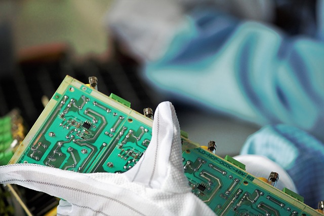
The printed circuit board (PCB) is a hard body that contains numerous electronic parts. It is typically greenish. In a procedure known as “PCB Assembling” or PCBA, these elements are glued onto the PCBs. The PCB is composed of a fiberglass base, elements, a copper sheet that creates traces, holes wherein the elements are installed, and levels that might be internal or exterior surfaces. It can produce multilayered PCB prototypes with up to 36 levels and mass-manufacture multi-layered PCBs assembling with 1-10 layers. The upper edges are present on both single-sided and double-sided PCBs, but there is no interior layer.
Solder masks are used to isolate the PCB substrate and elements, and epoxy resin is used to hold them securely. As with PCB colors, these soldering masks could be greenish, blues, or reddish. The elements would be able to avoid short-circuiting with the track or even other elements thanks to the soldering masking.
The copper trace on the PCB was utilized to transport electrical impulses from one location to another. Such transmissions could be discrete analog signals or high-speed digitized transmissions. That trace could be thickened to carry power/electricity and hence charge up equipment.
The parts are assembled on the PCB so that they can perform as intended. The PCB functioning is the most critical factor. Even when a simple SMT resistor is not carefully positioned or a small track is taken from the PCB, the PCB may never work. As a result, the elements must be properly assembled. Whenever elements are assembled on a PCB, it is referred to as PCBA or Assembling PCB. Depending on the parameters provided by the customer or users, PCB capability might be sophisticated or basic. PCB size ranges as well, depending on the demands.
A set of materials and devices is required for the assembling PCB. Here are a few of them:
- A Circuits Board: You’ll need the main circuit board to put the elements together.
- Electronic Systems: PCBs contain a wide range of complicated electronic systems, such as resistors, capacitors, diodes, transistors, and fuses.
- Soldering Substance: Solder is tin and leads to metallic elements that are molten and chilled to make a strong bonding.
- Soldering pieces of equipment: It will normally consist of waveform solder machines and soldered stations, as well as devices for surface-mount and through-hole technology (depending on which you’ll be using).
- Checking Instruments: It’s critical to evaluate your PCB to guarantee that it’s functional and prepared to ship.
You could start the PCB assembling procedure once you have all of your pieces of equipment and electric elements available. Surface-Mount Technologies and Thru-Hole Technologies are two sorts of technologies you can use based on the components you’ll be building.
Surface-Mount Technologies
Surface Mount Technology, or SMT, is a means of mounting smaller, more reactive parts such as transistors and diodes straight onto the PCB’s surfaces rather than using cabling. Surfaces Mounted Designs, or SMDs, are a kind of element that is commonly employed with this technique. There are 3 kinds of SMDs:
- SMDs that are not active (resistors, capacitors)
- ICs (Integrated Circuits)
- Diodes, transistor
Thru-Hole Technologies
Through Holes (or thru-hole) Technologies entails putting element leads or cables into drilled holes within PCB and putting those in. On either end of a Printed circuit board ( PCB, the additional cabling is connected to the pad). Through-hole elements are the most common application for this technique. There are two different types of Thru-hole elements:
- Axial Leading Component – elements with the lead that runs axial (in a straight line) across them.
- Radial Leading Components – elements with leads flowing from the same side rather than opposing ends.
PCB Assembly (PCBA) Procedures
Step 1: Utilizing a Stencil to Apply Solder Paste
First, add solder paste to the PCB board locations where the elements would be installed. Soldering paste is applied to the stainless steel stencils to accomplish this. A mechanized fixture holds the stencils and PCB connected, and the soldering solution is dispensed evenly to all of the board’s openings by the application. The solder paste is evenly distributed by the applicator. As a result, the appropriate amounts of soldering paste should be utilized in the application. The paste should continue in the targeted locations of the PCB assembly after the applicator is withdrawn.
Step 2: Automation Element Placing:
The automatic placing of SMT elements on PCB boards is the next phase in PCB assembly. Picking and placement robots are used to accomplish this. The designers prepare a file that will be fed to the autonomous robot at the designing levels. This file contains the preprogrammed X, Y measurements of all elements used with the PCB and indicates their locations. The robots would use this knowledge to precisely arrange the SMD gadgets on the boards. The parts would be picked up from the vacuumed grip and placed precisely on top of the soldering paste by the pickup and placement robotics.
Step 3: Soldering process
Soldering process solder is the third phase after the elements have been set and solder paste has been placed. The PCBs assembly and equipment are placed on the conveyor system belt during the reflow soldering procedure. This conveyor belt next transports the PCBs and materials into a large oven that is heated to 250 degrees Celsius. This temperature is sufficient to melt the solder. Melted solder would next be used to secure the elements to the PCB and form connectors. After the PCB has been exposed to extreme heat, it is placed in cooling. The solder junctions are subsequently solidified in a regulated manner by these coolers. This will make the connection between the SMT item and the PCB irreversible.
Step 4: Quality Control and Inspections
There was a risk that even after the soldering process soldering, the parts were misplaced because of a certain unintentional movement in the PCB retaining tray, resulting in a short circuit or open connections. These defects must be detected, and the procedure of doing so is known as inspection. Manually and automatic inspections are both possible.
Step 5: THT Components Fixation and Soldering
On several PCB assemblies, through-hole connectors were widely encountered. Plated thru Hole elements is another name for such components (PTH). The leads of these items would travel through the hole within the PCB assembly. Copper trace attaches these holes and vias to other holes and vias. When THT parts are put and bonded into such holes, they are electronically coupled to certain other holes on the same PCB as the circuitry. Because these PCBs could have both THT and SMD elements, the soldered methods described above for SMT elements, such as reflow solder, would not function with THT elements.
Step 6: Last Examination and Operational Testing
The PCB has become ready to be tested and inspected. This is a functioning test in which electrical impulses and energy are applied to the PCB at certain pins, and output is examined at specific test locations or output connections. This testing necessitates the use of typical laboratory tools such as an oscilloscope, a digital multimeter, and functional generating.
The testing verifies the functioning and electrical properties of the PCB, as well as current, voltages, analog, and digital signals, as specified in the PCB and circuits designs criteria.
Step 7: Completion, shipping, and last cleanup:
Now as the PCB has been thoroughly examined and determined to be in good working order in all areas, it’s time to remove any remaining flux, finger dirt, or oil staining. All forms of grime can be cleaned with a stainless steel high-pressure cleaning instrument and deionized water.
The PCB circuits would not be harmed by the deionized water. The PCBs are then dried with pressurized air after it has been washed. The finished PCB has become prepared to be packaged and shipped.
Interested in getting your PCB design done at affordable rates at JLCPCB, just visit us now at JLCPCB.COM.